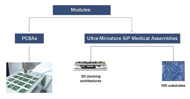
Advanced Packaging and Product Miniaturization Techniques
ON Semiconductor offers an array of technologies for medical applications where size, performance, and system integration are critical. ON Semiconductor has proven leadership in this field, addressing the highly space-constrained requirements of hearing aid manufacturers for over four decades. As other medical devices shrink in size, they too can benefit from miniaturization techniques.
Whether the need is for a custom component such as a complete tested PCBA or fully integrated SiP, ON Semiconductor offers custom packaging development and manufacturing services, from design and test through volume manufacturing.
Medical-Grade PCBA Modules
ON Semiconductor offers PCBA module design, manufacturing, assembly, and test services to the standards of quality and traceability demanded by medical device manufacturers.
Features like 2D barcodes laser marked onto every board for individual tracing is just one example of how our standard process is tailored to medical needs.
FDA Compliance
The ON Semiconductor facility located in Burlington, Ontario, Canada offers manufacturing compliance with the US Food & Drug Administration.
Ultra-Miniature SiP Medical Assemblies
ON Semiconductor has proven leadership in miniature System-in-Package (SiP) solutions, addressing the highly space-constrained requirements of hearing aid manufacturers for over four decades. As other medical devices shrink in size, they too can benefit from the same miniaturization techniques and assembles.
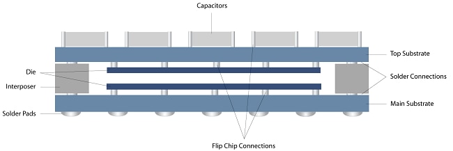
3D Stacking Architectures
Our custom 3D packaging connects different silicon die and discrete components together in the same package to dramatically save space and improve electrical signal performance by decreasing signal distances.
Our packaging techniques include:
- Stacking with or without wirebonds
- Modular, scalable architectures with high degree of manufacturing testability
- Mature, robust technologies and structures
- RoHS-compliant and ISO-certified
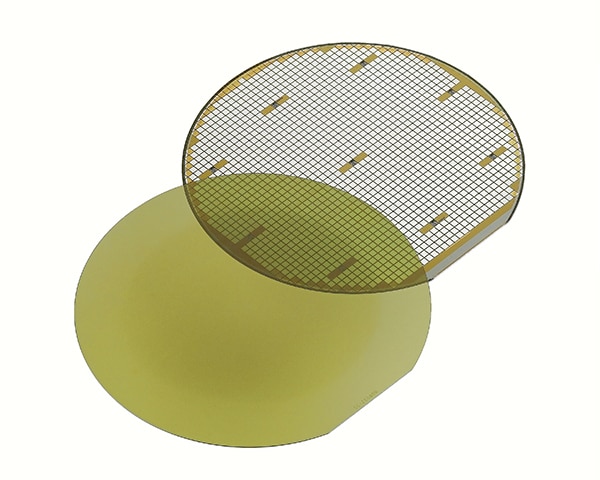
High Density Ceramic Substrates
ON Semiconductor fabricates high density, high performance ceramicbased substrate circuits to optimize miniaturization.
- Proprietary multi-layer double-sided thick film ceramic substrates
- High density interconnect (1 mil line/space geometries)
- Fine-pitch through-ceramic vias for 3D interconnection
- Excellent high frequency and thermal properties
- Low $ wiring density ratio provides excellent value proposition