Ever since electric vehicles (EVs) found their firm position on the automotive market, EV manufacturers have pushed towards higher power drivetrains, larger battery capacity and faster charging. To meet the demands of customers and extend driving range, EV manufacturers have been increasing energy capacity of a vehicle’s batteries. Larger batteries, however, mean longer charging time.
The most common charging methods are to charge from home overnight or at the workplace during the day. Both scenarios present different levels of power available to the EV. Drivers may not be able to fully charge their EVs overnight at home with a residential power outlet. At the workplace, a medium power AC charging station is likely available, but time at the charging station may become an issue if the car is equipped with a lower power on board charger (OBC). Increasing the OBCs power capacity provides more reasonable charging time but also increases system complexity and design challenges. While high power DC charging stations can rapidly refresh a battery to 80% of its capacity, this form of charging is not the norm.
To address both charge time and performance issues, many EV platforms are migrating from the current 400V battery pack to an 800V battery pack. When the vehicle is in drive mode, the higher available voltage can be utilized to increase electric motor power output or improve system efficiency while maintaining the same power level. In the charge mode, the higher battery voltage reduces the current required to charge the battery and can reduce charge time. Two crucial factors that impact OBC design are voltage and switching frequency. By increasing voltage and switching frequency, OBC capacities can be improved significantly. The system architecture must account for higher voltages which is why 1200 V devices become preferred thanks to their higher blocking voltage capability.
In addition to the trend toward 800V main battery packs, there is a parallel trend of increasing the power capability of the OBC. Units in the 6.6kW range were common in the past. Now many designs are 11kW (split phase mains) and 22kW (three phase mains). While this power level is often not supportable in the home, it is at the more than 126,000 AC charging stations currently available in the US. A higher power OBC can allow faster charge times while at work or in many public spaces, negating the need to establish a full charge while at home. As OBC power levels increase, the advantages of silicon carbide (SiC) MOSFETs also increases.
SiC-based components have proven advantageous in comparison to IBGT components when it comes to higher switching frequency applications. SiC technology continues to provide design benefits in the transition towards 800V batteries. OBC systems can be downsized and increase the overall “wall to wheel” efficiency.
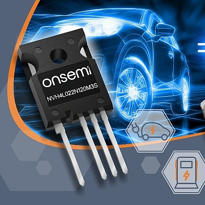
After the successful introduction of first generation 1200 V EliteSiC M1 MOSFETs, onsemi recently released its second generation 1200 V EliteSiC M3 MOSFETs that focus on optimizing the switching performance. M3S products are lined up 13/22/30/40/70 mΩ for discrete packages of TO247−4L and D2PAK−7L. NVH4L022N120M3S is auto-qualified MOSFET with the lowest RDS(ON) 22 mΩ at 1200 V.
The onsemi team has done extensive tests on key characteristics of M3S against M1. More details on how the evaluation was set up can be found in this application note. The M3S (NTH4L022N120M3S) requires less total gate charge QG(TOT) than M1 (NTH4L020N120SC1) which significantly reduces the amount of sinking and sourcing current from gate drivers, shown in Figure 1. The M3S has 135 nC at its recommended
VGS(OP) = +18V and 44% reduced FOM (Figure of Merit) factor in RDS(ON)*QG(TOT) than its older
M1 counterpart, meaning it needs only 56% of the gate charge for switching in the same RDS(ON) device.
The M3S also features better efficiency at lighter loads by storing less energy EOSS in its parasitic capacitances COSS than the M1 (Figure 2). Because the EOSS is dependent on the Drain−Source Voltage, not current, it becomes a critical loss for the efficiency at light loads.
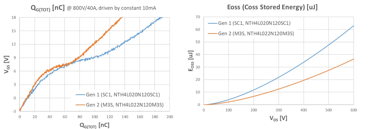
Figure 1. Total Gate Charge Figure 2.Eoss, Stored energy in Coss
Switching losses are critical parameter in system efficiency. Figure 3. shows the switching performance where M3S achieved much improved switching performance at the given conditions, 40% lower in EOFF, and 20−30% lower in EON, 34% lower in the total switching loss than M1. In high switching frequency applications, it will cancel the disadvantage of the higher RDS(ON) temperature coefficient.

Figure 3. Inductive Switching Losses
Increasing switching frequency helps designers to reduce the size of energy storage components such as inductors, transformers and capacitors, resulting in smaller volume of the system. More compact size and higher power density enable smaller package size for the OBC system, which gives engineers further options to budget additional weight elsewhere in the vehicle. Furthermore, operating at a higher voltage also reduces the current required throughout the vehicle, leading to lower cable costs between the power system, battery, and OBC.
To learn more about our EliteSiC MS3 MOSFETs and the benefits of utilizing SiC for your next OBC design, join our technology webinar: Adopting Silicon Carbide for OBC and DC/DC Power Conversion. We will take a closer look at comparison between SiC MOSFETs, IGBTs and silicon super junction MOSFETs for OBC application.