Silicon carbide (SiC) is a new wide-bandgap (WBG) material that is coming to the fore, especially in challenging applications. However, as it is new (and despite significant information being available online) there are many myths preventing designers from using the technology to its full potential.
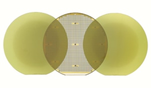
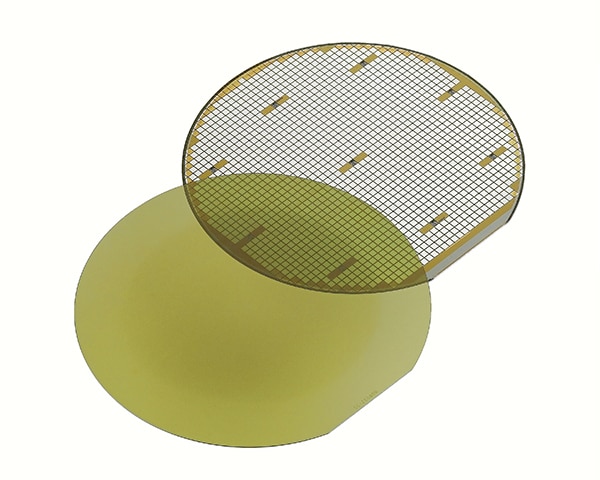
Figure 1: SiC Wafer Image
Some think that gallium nitride (GaN) is the preferred alternative to silicon MOSFETs, and SiC is purely an IGBT replacement. However, SiC has an excellent RDS(ON)*Qg figure-of-merit (FoM) and low reverse recovery charge (Qrr) making it an excellent choice in hard switching apps such as Totem Pole PFC or a synchronous boost.
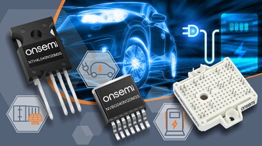
Figure 2: onsemi 1200 V EliteSiC M3S Fast-Switching MOSFETs and Half-Bridge Modules with Industry’s Lowest Rds(on)
Compared to IGBTs, SiC MOSFETs have better avalanche ruggedness and in the event of a short circuit, when used with an appropriate gate driver, SiC can be at least as rugged as IGBTs.
The extensive use in electric vehicle (EV) traction applications that operate at 10-20kHz might lead some to believe that SiC is a low-frequency technology. However, reductions in the die area resulting in lower gate charge (Qg) mean that SiC devices are used successfully in Totem-Pole PFC (TPPFC) at 100 kHz and soft-switching LLC at 200-300 kHz.
Clearly, driving a SiC device does require a different approach to silicon. The need for a negative turn-off gate voltage is not wholly true, in some applications with good layout practices, it has been shown to be not necessary. However, to be sure to eliminate inadvertent turn-on due to “bouncing,” using a negative gate drive is considered by many to be good design practice.
SiC gate drivers are available and simple to use. The perception that they are complex probably arose from engineers trying to drive SiC devices with Si MOSFET or IGBT drivers. Dedicated SiC drivers offer convenient features such as negative gate drive, Desaturation (DESAT), Over Current Protection (OCP), Over-Temperature Protection(OTP) and other protections. When using the right driver, driving SiC is as easy as driving a silicon MOSFET.
Often, SiC is considered expensive and if a highly simplistic device-to-device comparison is made, comparing a silicon MOSFET to an equivalent SiC device, then there will be a small price premium for the SiC device. However, the enhanced performance of SiC devices drives significant cost savings elsewhere in designs that more than offsets this small premium.
If we consider a generic silicon-based 30 kW power solution, then we find that 90% of the overall cost relates to the inductors and capacitors (60% and 30% respectively), with the semiconductor devices representing only 10% of the overall BOM cost. Replacing the silicon MOSFETs with SiC switches allows capacitance and inductance to be reduced by 75%, bringing a substantial size and cost reduction, far outweighing any cost premium for the SiC devices.
Following graphic shows at a high level how higher SiC enables higher breakdown voltage devices with excellent Rds(on)*Qg characteristics allows simpler topologies to run at higher frequency thereby enabling cost and size reduction.
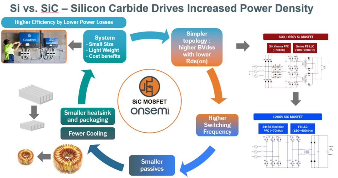
Additionally, as SiC operates more efficiently, heatsinks are significantly reduced (or eliminated) giving a further size and cost reduction. As a result, the total BOM cost of a SiC design has reached a point where it is more favorable than the equivalent silicon approach.
While SiC remains a relatively new technology, its ecosystem has developed rapidly as SiC becomes mainstream. Suppliers offer many SiC devices and associated gate drivers, in various packages to suit many applications, along with reference designs, application notes and simulation models/tools. onsemi offers a powerful suite of online modeling and simulation tools. The online Self-Service PLECS Model Generator allows users to generate a high fidelity PLECS model of their custom circuitry. This model is then uploaded into the Elite Power Simulator where onsemi’s power products can be introduced to showcase system performance including effects of semiconductor process corners. This virtual environment enables system designers to rapidly iterate toward optimized solutions before committing to hardware, thereby significantly reducing the time to market.

The supply chain is also evolving - following onsemi’s recent acquisition of GT Advanced Technologies (GTAT), the only large-scale supplier with end-to-end supply capability, which includes volume SiC boule growth, substrate, epitaxy, device fabrication, best-in-class integrated modules and discrete package solutions (Learn more about End-to-End SiC Manufacturing Capabilities and EliteSiC Family Solutions Advance a Sustainable Future).
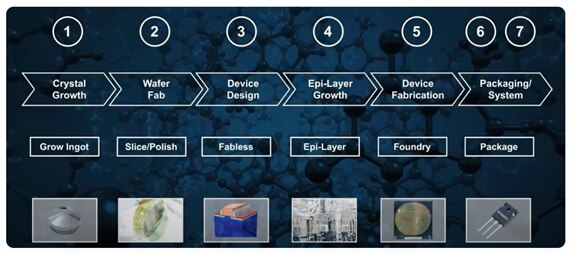
Figure 4: onsemi’s End-to-End Supply Chain
onsemi will rapidly grow the capacity of substrate operations fivefold and make substantial investments in expanding the company’s device and module capacity, quadrupling by 2024, with the capability to double capacity again in the future.
While many myths persist, asking the right questions and dispelling these myths will allow designers to realize the full potential of this new material.
Learn more about onsemi’s EliteSiC.