Providing power to today’s high performance image sensors has become more challenging than in the past. With the increased pixel size and refresh rate it has brought new challenges in the power delivery solution for the engineer responsible for the camera module. There are three key factors to consider when designing an image sensor power solution.
PCB Layout and Capacitor Selection
The image sensor is a highly dynamic device that requires an optimized system solution of the voltage regulator, output capacitors and PCB routing/placement. A similar design done with the same components can provide drastically different results. (See Figure 1) The MARS reference design showcases the proper PCB layout and placement of components in order to achieve a clean power delivery system.
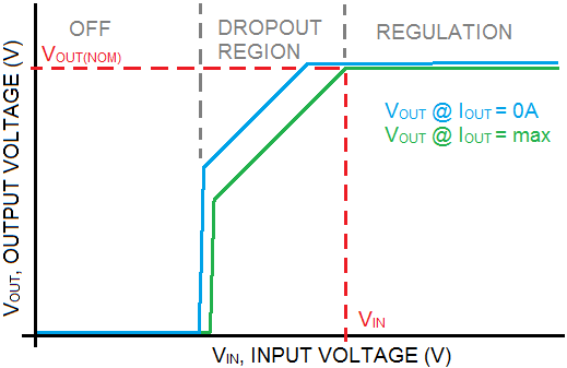
Figure 1 – Voltage Ripple on Vdd due to poor PCB layout and capacitor placement
The selection of the output capacitor must take into consideration LDO stability, hold up charge during transient response and start-up interval/overshoot.
PSRR Impact
PSRR describes how a signal on the DC input voltage of a regulator system is transmitted to the regulated output. This is especially important in an image sensor application as any noise injected into the system translates into image quality degradation. As we can see in Figure 2 below the PSRR of the system less than 100kHz is controlled by the selection of a proper LDO. Above 100kHz the PSRR is controlled by the proper selection of passive components and PCB layout/placement. In this example you can see how a High PSRR LDO like the NCP163 (NCV8163) provides >85dB response up to 10kHz and >45dB up to 1MHz.
Figure 2 – PSRR System Response and PSRR Response of NCP163 LDO (High PSRR)
In Figure 3 below you see a comparison of a traditional DC-DC converter versus a High PSRR LDO. The DC-DC has inherent switching ripple on the output due to the topology used to increase efficiency. This ripple is transferred to the image sensor and seen as image quality degradation. In order to achieve high efficiency and maintain the performance of a High PSRR LDO a new bias rail architecture is also available in products like the NCP134 (NCV8134). This bias rail configuration allows you to maintain the High PSRR performance capability but provides a higher efficiency solution.
Figure 3 – Image Quality and Ripple Comparison between an LDO and a DC-DC Converter
System Noise
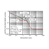
There are two main sources of noise at the output of the LDO. One is external parts coupling to the input of the LDO which is address above with High PSRR solutions. The second is noise generated by the internal LDO circuitry. In order to address this requirement new generation LDO products offer ulta-low noise performance and the ability to optimize the spectral density with an external capacitor. The NCP705 (NCV8705) is used on the MARS reference design to generate the 2.8V supply the noise sensitive rails of the image sensor and co-processor.
Figure 4 – Output Voltage Noise Spectral Density with Varying Feedforward Capacitor Values
By following a few simple rules, and utilizing the MARS reference design as a guideline, designing a Clean Power solution should be fairly straight forward. A little investment in understanding the design approach will enable you to realize the best image quality in your end product.